As the power density of semiconductor components, such as high-power LEDs and laser diodes (LDs), continues to increase, the thermal management and interconnection demands of high-power, high-density, and high-frequency devices have become increasingly critical. Lincotec has successfully applied its sputtering process technology to develop high-performance advanced heat dissipation substrates. These advanced heat dissipation substrate solutions are specifically designed to drive key applications in future technological advancements, playing an indispensable role in fields such as industrial lasers, optical communications, sensors, and medical laser modules.
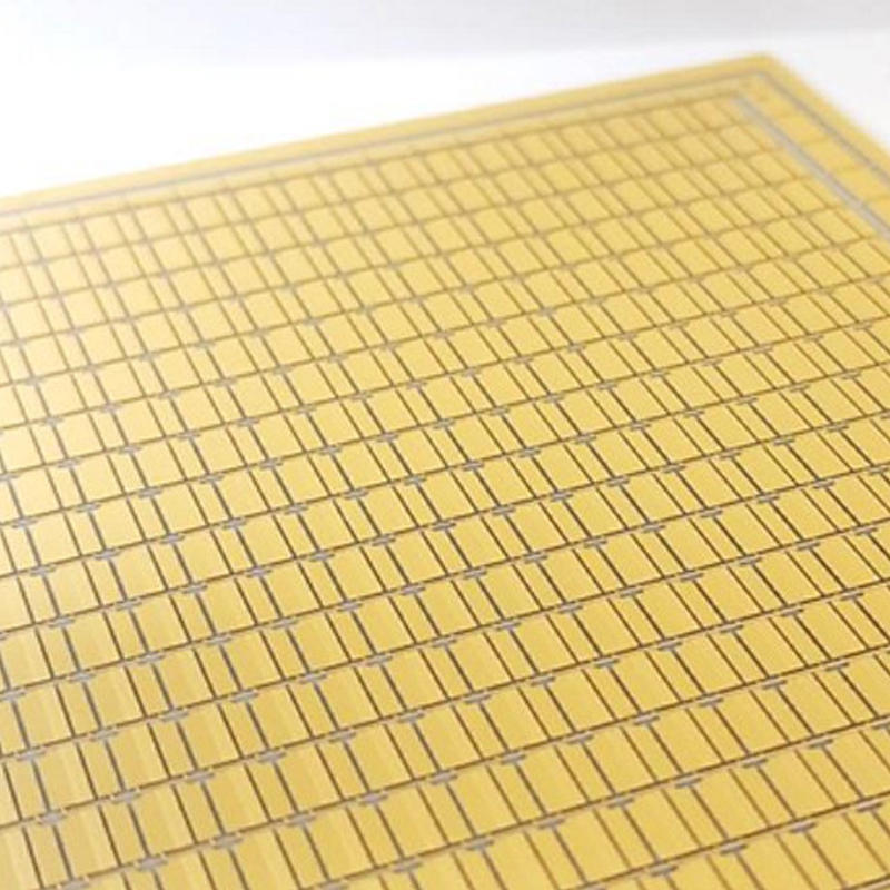
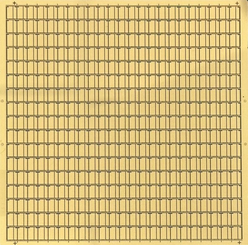
Lincotec’s core strength lies in its vertically integrated capabilities, spanning equipment to manufacturing processes. This enables the production of precise metallized circuits on various substrate materials, including Alumina, Aluminum nitride (AlN), and Silicon Carbide (SiC). These substrates meet the design requirements for miniaturization and high integration of high-power components while delivering exceptional thermal conductivity, insulation, and reliability.
A key differentiator is Lincotec’s advanced thermal substrate manufacturing process, which leverages proprietary sputtering equipment that has achieved the top market share in the semiconductor system-in-package (SiP) sector. By combining sputtering, plasma etching, and years of mass production expertise, Lincotec has established a fully integrated supply chain from equipment to foundry services. This enables significantly reduced product development timelines for clients while ensuring consistent quality and production capacity. With its deep expertise in coating technology, Lincotec offers highly flexible customized foundry services, with primary product categories including thick film and thin film solutions, confidently providing clients with the most comprehensive thermal management solutions.
| Item | Thick Film | Thin Film | |
|---|---|---|---|
| Product Image |
|

|
|
| Applications | IndustrialLasers, Optical Communications, Sensors, Medical | ||
| MultilayerFilmStructure |

|

|
|

|
|||
| Substrate | |||
| Material | AlN(170, 200, 230W/mK) | AlN(170,200,230W/mK) | |
| SiC(280, 380W/mK) | SiC(280, 380W/mK) | ||
| Thickness | 0.3~0.4mm; 0.15~0.3mm(customized) | 0.15~0.4mm | |
| Size | AlN: 4.5"x4.5" panel | 2"x2" panel | |
| SiC: 6" wafer | |||
|
Metal Layer |
|||
| Matel content | Cu/Ni/Au: 30~80μm/>1μm/>0.5μm | Ti/Pt/Au=0.06~0.1μm/0.2μm/0.3~1μm | |
| Metal thickness | Cu: 30~100μm ±15μm | Ti/Pt/Au: 0.1μm/0.2μm/1μm ±10% | |
| Pattern | L/S=100/150μm (Cu thickness>50μm | L/S=30/30μm | |
|
Bonding Layer |
|||
| AuSn thickness | 2μm~6μm±10% | 2μm~6μm±10% | |
| AuSn content | Au/Sn:75/25±5wt% | Au/Sn:75/25±5wt% | |
| Others | |||
| Dicing | ±50μm(std); ±15μm (special spec.) | ±50μm(std); ±15μm (special spec.) | |
| Reference model | 4558/4550/4048 | 0707/0912/0407/0808 | |
| Capacity (per month) | 7k~30k (4.5"x4.5" panel) | 1k (2"x2" panel) | |
Lincotec provides high-quality advanced coating foundry services to our clients. Our experienced team delivers tailored processing and manufacturing solutions to meet your precise specifications. Whether for small-batch prototyping or mass production, we ensure timely delivery of products that fully satisfy your requirements.
For prototyping or mass production needs, please reach out to us. We are committed to delivering exceptional solutions. Kindly visit the “Contact Us” page on our official website to submit your contact details and a brief overview of your coating foundry requirements. Lincotec will promptly respond, assess the feasibility of your project, and actively engage in partnership discussions to foster successful collaboration.