
As the popularity of smartphones, tablets, and other portable devices continues to rise, the demand for lightweight, slim, and high-performance electronic products is also on the rise. With the shrinking of linewidth and line spacing, there is growing limitation on the size and shape of circuits. This has inspired developers of forward-looking technologies to continuously explore more precise, efficient, and cost-effective process technologies.
By implementing Lincotec's high-selectivity and high-uniformity etching technology, excess metal materials can be accurately removed without damaging other parts, enabling the generation of precise circuit patterns. Furthermore, the integration of high-performance thin-film sputtering equipment addresses issues like metal adhesion and coating uniformity, thus improving product yield and competitiveness.
Application Description
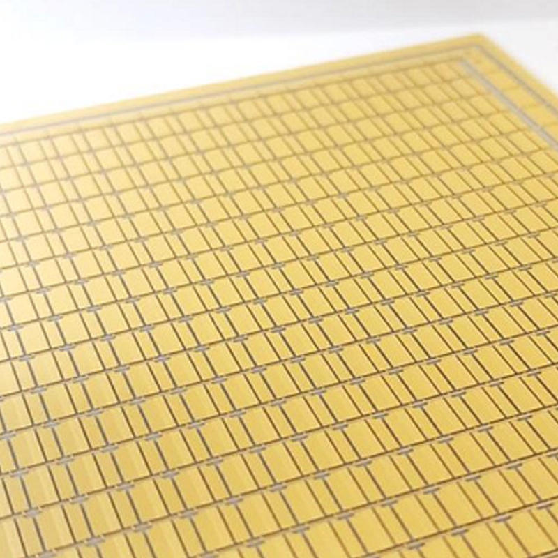
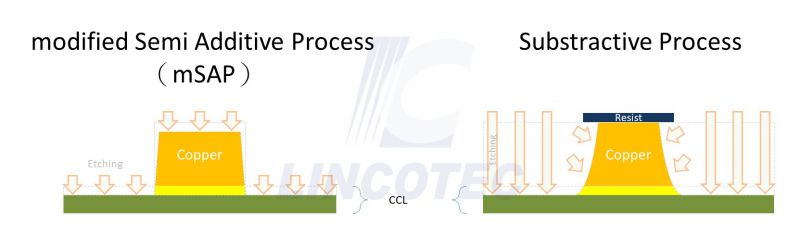
Currently, there are three primary circuit manufacturing processes for advanced substrates and high-end PCBs: Subtractive Process, Additive Process, and modified Semi Additive Process (mSAP).
Subtractive Process is a proven practice to remove the unnecessary copper layer on the surface of the Copper Clad Laminate (CCL) and create the circuit board. However, this method can have issues with side etching during the etching process, which can lead to yield problems, especially with smaller line width and spacing.
Additive Process is the opposite of Subtractive Process. It involves creating copper circuit patterns directly on a non-copper base substrate using exposure and development, followed by chemical copper plating to achieve the required thickness. While additive processes are better suited for creating fine circuits, the equipment setup costs are higher. Additionally, the use of different substrate materials can result in a longer learning curve and higher technical barriers.
Modified Semi Additive Process (mSAP) combines features of both additive and subtractive methods. It uses a thinner copper foil layer on the base substrate. Initially, a photoresist mask is applied to the copper foil base substrate, and circuit patterns are created by exposure and development, exposing the underlying copper foil layer. Then, copper plating is used to increase the thickness of the copper layer in the circuit areas. Finally, the photoresist layer is removed, and excess copper foil is etched away. Since mSAP uses a thinner copper foil layer on the base substrate, the etching process is shorter, reducing the risk of side etching issues. Therefore, mSAP can be used to create smaller circuit patterns, achieving higher circuit performance efficiency compared to subtractive methods.
With the proliferation of smartphones, tablets, and other portable devices, the demand for lightweight, thin, and high-performance electronic products has been on the rise. As line widths and line spacing continue to shrink, there are greater limitations on the size and shape of circuits. This drives developers of forward-thinking technologies to explore more precise, efficient, and cost-effective process technologies. Incorporating Lincotec's high aspect ratio and high uniformity etching technology allows for the accurate removal of excess metal materials without damaging other parts, enabling the creation of precise circuit patterns. Furthermore, by integrating high-performance thin-film sputtering equipment, issues related to metal adhesion and coating uniformity can be resolved, and high-capacity production can enhance product yield and competitiveness.
Lincotec holds proprietary intellectual property and can collaborate with customers in process development and experimental validation. In particular, in the applications of redistribution layer (RDL) processes, the company has rich experience in various techniques such as Desmear, Descum, Ti etching, and Seel layer sputtering, etc. In addition to offering sampling services in the R&D phase with different process formulations, Lincotec has qualified and highly precise laboratories for sample testing.