Advanced Packaging Beyond Moore's Law
In response to the demands of emerging technology products such as artificial intelligence, high-speed communication technologies (5G, Wifi 6), efficient data centers, and automotive electronics, etc., achieving high transmission speeds, high signal quality, and low latency in packaging technology is of foremost importance. This relies on the use of advanced materials and continuous improvement in process equipment capabilities to break through to finer overall production processes. Furthermore, the new generation of process equipment not only needs to meet performance requirements but also address environmental concerns, as a part of the company's sustainability efforts.
Lincotec's thin film sputtering and plasma etching platforms, with dry and eco-friendly processes as their technological core, not only meet customer requirements in terms of equipment capabilities but also provide customized automation platforms, ensuring high yield, high productivity, and the lowest Cost of Ownership (COO). In the field of advanced semiconductor packaging, we possess expertise and capabilities in the following equipment applications and have a strong professional competence that can be extended to other process applications through similar process modes.
Every electronic component or its system generates a certain
level of electromagnetic interference (EMI) during operation, which can have an adverse
impact on the performance of surrounding electronic devices. Therefore, it is essential
to limit EMI from electronic components or their systems and ensure immunity to
interference in the environment.
"EMI Shielding Sputtering" involves using a dry process to physically deposit
a sufficient thickness of shielding material on the exterior of electronic components to
achieve electromagnetic shielding.
In the post-Moore's Law era, the development of front-end processes and equipment
costs have significantly increased. To further enhance chip integration and reduce
manufacturing costs, the adoption of advanced packaging is an evolutionary trend in the
semiconductor industry.
Fan-out packaging technologies, including FOWLP and FOPLP, share a common
characteristic, allowing the formation of a greater number of I/O pins in a fan-out
fashion. This enables a single chip to integrate more functions and achieve benefits
such as thinness and cost reduction. The main difference between the two lies in the
choice of the carrier used during production, which needs a balance between the fine
line size and packaging cost based on the chip's application purpose.
"Know Good Die (KGD)" manufactured via advanced semiconductor process
technology typically has higher circuit density. However, it's necessary to
rearrange the connection points (I/O Pads) from the narrow area on the surface of the
bare die outward via fan-out technology to facilitate subsequent chip assembly.
The Redistribution Layer (RDL) involves using wafer-level metal wiring technology to
extend the connection points to the outside of the chip, simultaneously achieving a
thinner packaging thickness and superior electrical performance.

As the popularity of smartphones, tablets, and other portable devices continues to rise,
the demand for lightweight, slim, and high-performance electronic products is also on
the rise. With the shrinking of linewidth and line spacing, there is growing limitation
on the size and shape of circuits. This has inspired developers of forward-looking
technologies to continuously explore more precise, efficient, and cost-effective process
technologies.
By implementing Lincotec's high-selectivity and high-uniformity etching technology,
excess metal materials can be accurately removed without damaging other parts, enabling
the generation of precise circuit patterns. Furthermore, the integration of
high-performance thin-film sputtering equipment addresses issues like metal adhesion and
coating uniformity, thus improving product yield and competitiveness.
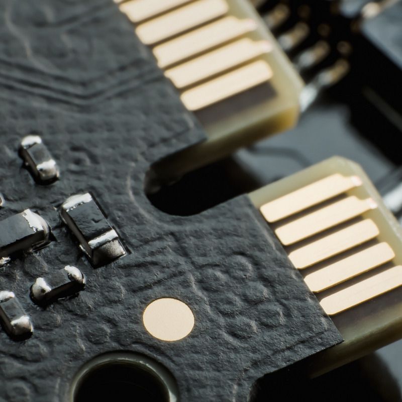
Non-Plating Line (NPL) Plating Technology offers a method that doesn't require the installation of plating wires on the substrate's surface. It allows for the electroless nickel-gold plating of contact pads at the edge of the substrate. The main approach involves using a conductive film as the current conduction path to connect various contact pads on the substrate, enabling the electroless nickel-gold plating and structure. This significantly reduces the impact caused by the installation of plating wires.
Backside metallization is a process used in the manufacturing of electronic devices where
one or more layers of metal are deposited on the backside of a semiconductor substrate
(such as a silicon wafer) or an integrated circuit (IC) using vacuum sputtering. These
metal layers can serve as bonding/heat-conducting layers and can also bond with the
substrate to improve heat dissipation, provide electromagnetic shielding, and reduce
resistance.
The quality of the sputtering process in backside metallization has a significant impact
on product yield and the reliability of semiconductor components. Poor bonding of the
metal layer to the product can lead to issues like delamination and increased impedance.
Low-ohmic contact resistance and excellent thin film adhesion are critical requirements
for the backside metallization process.

Compared to cored substrates, coreless substrate technology eliminates the fiberglass
cloth used as the core layer and uses layer-to-layer insulation materials directly for
wiring and packaging.
Coreless substrate technology reduces costs by eliminating the core layer. Additionally,
the improved wiring capability allows for minimal limitations in the arrangement of
solder ball bumps and achieves excellent high-speed transmission characteristics,
improving both AC and DC power performance.