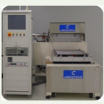
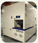
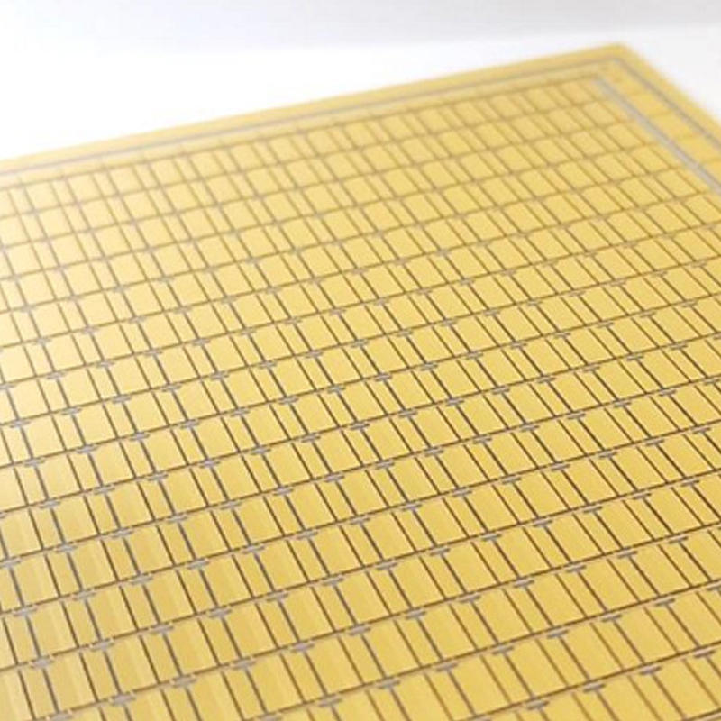
Since its application in semiconductor manufacturing in the 70's, plasma etching technology has become a crucial core technology in the industry. Compared to wet etching processes that may have water pollution issues, dry plasma etching technology is more in line with modern green manufacturing requirements. Its applications have gradually extended to various fields, including advanced packaging, PCB manufacturing, optoelectronics, Micro LED, MEMS (Micro Electro Mechanical Systems), etc. To meet the requirements of modern micro-scale circuits and high electrical performance, the control of plasma sources, design and simulation of electric fields, and process formulation including processing gas ratio have become increasingly complicated. This has been forming an industry that demands deeply accumulated knowledge and experimental data, highly relies on prototype testing and sample analysis before mass production. The following is a brief description of Lincotec's plasma processing equipment capabilities:
- Surface Cleaning/Metal Oxide Reduction
- This process involves placing materials in a vacuum chamber and using charged ions generated by plasma (such as Ar+) to remove contaminants or oxide layers from the material surface. This is followed by vacuum pump extraction to achieve material surface cleaning or oxide layer removal.
- Surface Activation/Surface Modification
- This is a method of using plasma technology to induce chemical reactions on the material surface to improve its surface properties. For instance, to enhance surface adhesion, charged ions generated by plasma are used to bombard material surface, change surface molecular structure, and increase surface adhesion and affinity.
- Descum/Photoresist Stripping
- In the exposure and development process, a photoresist stripper is used to remove unnecessary photoresist agents. However, there may still be residues from partially removed photoresist on the material surface. These residues could potentially interfere with the subsequent pattern resolution of circuits, thereby affecting product performance. Plasma etching is an effective method for removing residual films. It operates in a high vacuum condition, with critical techniques including specific process gases, specific plasma power supply control methods and parameters, and excellent electric field configuration, to generate highly isotropic plasma or saturated and uniformly distributed free radicals, which further physically breaks down or chemically removes contaminants from the material surface. This method offers advantages such as high efficiency, environmental friendliness, and high reproducibility, ensuring the reliable progress of subsequent processes.
- Desmear/Etch Back/Via Formation/Trench Formation
- When lasers or other methods are used to generate vias or trenches in the material during the PCB manufacturing process, adhesive or carbon residues may still remain. Desmear process of plasma etching equipment, with its high selectivity characteristics, is capable of properly removing residues from the bottom and sides of holes or trenches, and can further remove some dielectric layers on the walls of holes or trenches and etch back and expose the copper layer, ensuring good copper adhesion to the walls of holes or trenches and excellent electrical performance.
- High Aspect Ratio Application
- Lincotec’s proprietary hardware configuration, combined with advanced control methods, effectively minimizes material deformation caused by variations in incoming material conditions or temperature changes. This ensures that the etching material maintains excellent flatness, and when assisted with a high-energy plasma source and high non-isotropic electric field control, results in excellent high-aspect-ratio etching.
- Metal Etching
- When a process requires removal of metal layers on material surface, such as a seed layer, due to the crystalline characteristics of metal atoms, physical plasma etching alone is not effective in removing them, and may potentially damage the underlying material during removal. Therefore, it is crucial for removing metal to be assisted with chemical plasma etching technology. Lincotec has proprietary process formulations that work with different treatment methods suitable for different metal materials, achieving excellent etching performance.
- Dielectric Thin Down
- When continually striving to reduce package sizes, apart from reducing line width and line spacing, thinning the ABF material to make it thinner is a common practice. Lincotech’s chemical plasma etching equipment is tailored to meet the requirements of this process, enabling the achievement of uniform dielectric layer thinning.
- Remove Sacrificial Layer
- In MEMS manufacturing, due to structural characteristics it often requires a sacrificial layer, to be initially set up and then removed to create gaps once the three-dimensional structure of metal layer is formed. However, the sacrificial layer is usually covered by the metal layer. Selecting appropriate process gases and employing a high-selectivity etching method to remove the sacrificial layer can achieve the purpose of this process.
In this aspect, Lincotec possesses independent intellectual property and abundant experience in process development, as well as expertise in the key technologies of plasma etching, such as ICP, CCP, RIE, HDP, RPS, ESC, etc. We also have an independent formulation knowledge database, allowing us to select the appropriate processes based on material characteristics. We can collaborate with customers on process development and experiment validation. In addition to offering sampling services in various process stages during the research and development phases, we have qualified and highly precise laboratories for sample testing.
Product Series PISCES® Family
| Model |
PC series |
PD series |
PE series |
PF series |
| Schematic |
 |
 |
 |
 |
| Application |
Surface cleaning
Surface modification
Surface activation
Metal oxide reduction |
Desmear
Descum
Metal etch
Oxide etch
Surface shape control |
Dielectric thin down
Etch back
PR stripping
Remove sacrificial layer |
Via formation
Trench formation
High AR desmear
Fine line etching |
