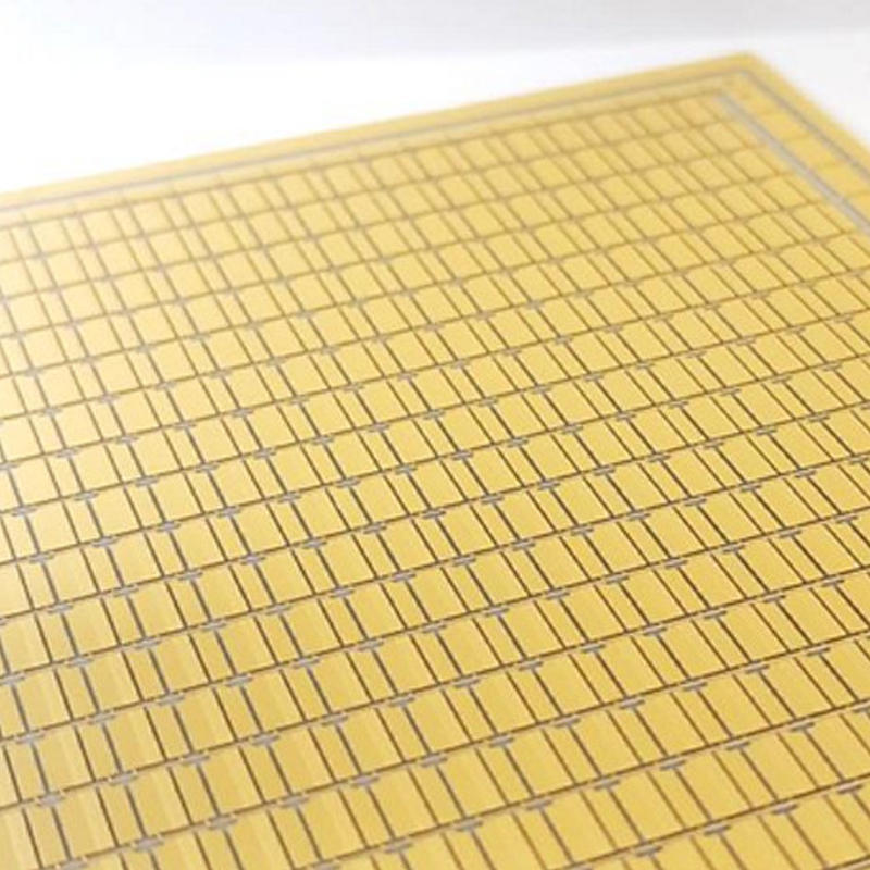
Thin film sputtering process is a technology that creates a uniform film of metals (including pure metals and alloys) or non-metal materials (such as silicides, carbides, nitrides, and oxides) on a substrate in a vacuum environment by using a plasma source. Typically, a voltage difference is generated between the two ends of electrodes, creating an electric field, which dissociates the process gases (e.g. argon) into a plasma state that bombards the target material. This physical vapor deposition (PVD) mechanism enables the material on the target to adhere uniformly to the substrate, forming a thin film. Lincotec specializes in thin film sputtering technology and offers a variety of equipment configurations to meet diverse processing requirements:
- Inline Sputter:
- Unlike cluster-type deposition equipment, which arranges vacuum chambers radially and may result in inefficient unused space between adjacent chambers and potential risk of difficult maintenance in the center when the size of the plated object is large (e.g. 700mm x 700mm). Linear continuous deposition equipment connects chambers in a linear manner, minimizing unused space and facilitating operation and maintenance. This configuration is more suitable for medium to large substrates.
- Horizontal Sputter:
- This is the most common deposition method, where the substrate is placed horizontally, and the deposition surface is typically facing upwards. The opposite side of the deposition surface can be effectively temperature controlled with the help of cooling modules. In this configuration, the target material is typically located above the chamber, making it easier for replacement and maintenance.
- Vertical Sputter:
- In contrast to horizontal sputter, which is typically used for single-sided deposition, vertical sputter positions the substrate vertically. It is suitable for double-sided deposition or large substrates, but usually requires the use of specialized fixtures for handling and minimizing substrate deformation. If additional temperature control is required, a specially designed automatic cooling mechanism is necessary, making the structure more complex.
- Roll-to-RollSputter:
- Roll-to-roll (R2R) deposition refers to continuously depositing films on thin and flexible substrates, such as polymer films (e.g., PET, PP, and PI films), metal foils, or flexible ultra-thin glass, after the substrate is rolled and fed into the thin-film deposition equipment for continuous deposition.
Additionally, in the field of thin film sputtering, Lincotec has the capabilities in key components and modules and automation integration, such as plasma field simulation, surface pretreatment function modules, plasma etching function modules, vacuum ovens, reflow function modules, rotating target modules, low-temperature deposition modules, anti-warping modules, equipment front-end modules (EFEM), and SECS/GEM modules, etc.
Furthermore, Lincotec holds independent intellectual property rights and extensive process development experience. There is an independent knowledge base that allows the selecting suitable process configurations based on material characteristics. The company can collaborate with customers for process development and experimental verification. In addition to providing sampling services in various process formulations during the R&D stage, the company also has a qualified and highly precise laboratory for sample testing.