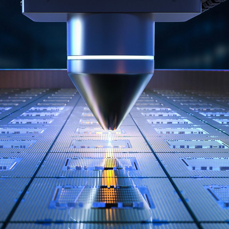
"Know Good Die (KGD)" manufactured via advanced semiconductor process
technology typically has higher circuit density. However, it's necessary to
rearrange the connection points (I/O Pads) from the narrow area on the surface of the
bare die outward via fan-out technology to facilitate subsequent chip assembly.
The Redistribution Layer (RDL) involves using wafer-level metal wiring technology to
extend the connection points to the outside of the chip, simultaneously achieving a
thinner packaging thickness and superior electrical performance.
Application Description
With advancements in miniaturization technology and the increasing complexity of chip functions, "Know Good Die (KGD)" manufactured with advanced semiconductor processes has extremely high transistor density and line density. However, it becomes impossible to accommodate all the pins within the area of a bare die. Therefore, the rearrangement of connection points (I/O Pads) from the surface of the bare die to the outside through fan-out technology is required to meet packaging and other circuit requirements.
The technology that redirects the metal wire connection points is broadly referred to as Redistribution Layer (RDL) technology. In applications, this can be further categorized based on line width and space (L/S) into:
(1) Ultra-fine line applications by wafer fabs. (2) Fine line applications by advanced packaging facilities. (3) Fine line applications by advanced substrate plants.
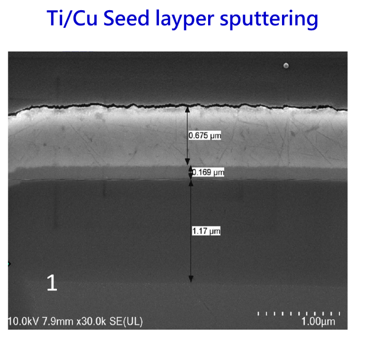
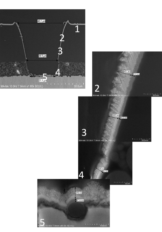
Different process solutions are employed in various applications to create metal lines. For example, ultra-fine lines can be produced using photomasks through exposure, development, and etching, or alternatively, laser lithography can be used in combination with cleaning, sputtering a metal seed layer, electroplating to thicken the metal layer, and etching to remove the seed layer to create thin metal lines on the substrate. The former can achieve ultra-fine line applications but has higher equipment costs, which are more common in wafer fabs. The latter approach is typically used in packaging facilities or substrate plants.
Furthermore, in response to ESG policies, the latter has gradually transitioned from wet processes to dry processes. For example, dry plasma etching has been employed for substrate cleaning instead of wet cleaning. The method of etching to remove the seed layer has also shifted from wet processes using chemicals to dry plasma etching to achieve lower material consumption, reduced environmental pollution, and simplified post-processing.
The diagram below illustrates the Die-First/Face-up Redistribution Layer (RDL) process used by advanced packaging facilities with Ajinomoto Build-up Film (ABF) as the substrate:
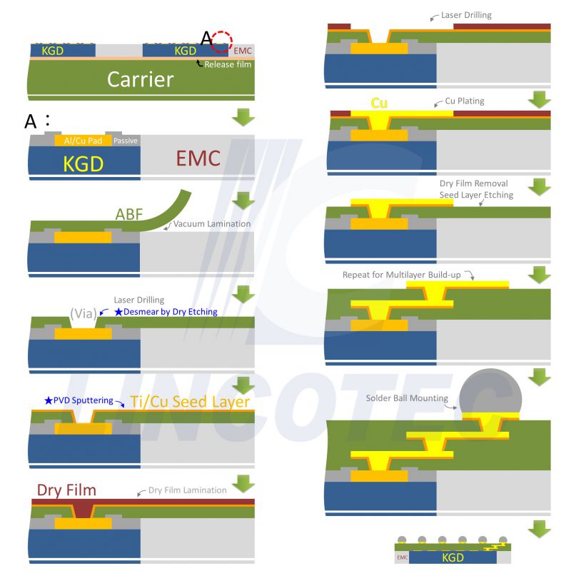
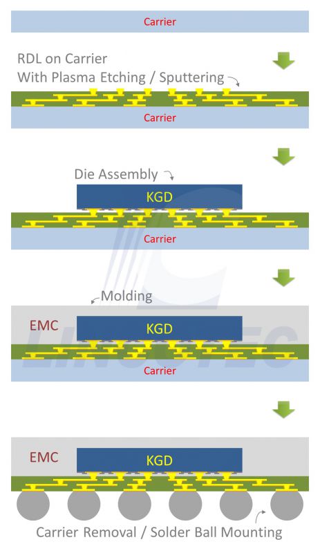
In the Die-First process, known good dies (KGD) are first placed directly, followed by the RDL process. However, this process carries the risk of damaging KGD due to process yield issues. Therefore, there is another Die-Last process, where RDL is completed first, and then KGD is attached, as shown in the diagram below. While this approach requires using a carrier as a temporary carrier, followed by its removal and the attachment of solder balls on the same side, making the process slightly more complex compared to Die-First, it effectively prevents KGD loss.
Lincotec possesses proprietary intellectual property and can collaborate with customers in process development and experimental validation. Especially in the applications of RDL processes, the company has extensive experience with technologies like Desmear, Descum, Ti etching, and Seel layer sputtering, etc. In addition to offering sampling services in the R&D phase with various process formulations, Lincotec has qualified and highly precise laboratories for sample testing.
Lincotec Features
Specialized in Sputter and Etching technologies, mastering key capabilities for RDL.
Achievements