In the post-Moore's Law era, the development of front-end processes and equipment
costs have significantly increased. To further enhance chip integration and reduce
manufacturing costs, the adoption of advanced packaging is an evolutionary trend in the
semiconductor industry.
Fan-out packaging technologies, including FOWLP and FOPLP, share a common
characteristic, allowing the formation of a greater number of I/O pins in a fan-out
fashion. This enables a single chip to integrate more functions and achieve benefits
such as thinness and cost reduction. The main difference between the two lies in the
choice of the carrier used during production, which needs a balance between the fine
line size and packaging cost based on the chip's application purpose.
Application Description
Traditional Moore's Law is often interpreted as follows: the number of transistors that can be
accommodated on a unit area of an integrated circuit roughly doubles every two years. Similarly, the
price of chips with the same computing speed is halved every two years. However, with the gradual
physical limits reached by foundries in their advanced front-end manufacturing processes and the
immense capital investment required, the pursuit of miniaturization in the front-end processes is no
longer the sole means of the semiconductor industry.
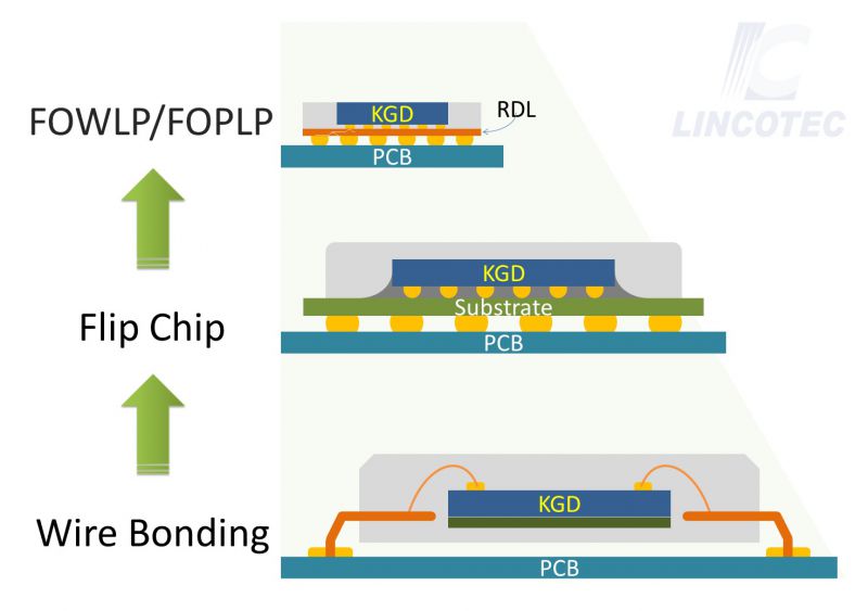
The development of advanced packaging processes, from early wire bonding technology, flip-chip technology, to the current fan-out packaging technology, involves continuous efforts to enable chip stacking and reduce the spacing between adjacent chips. This shortens the distance of metal interconnects (Interconnect) between chips, thus reducing size and signal transmission distances for improved electrical performance.
To achieve this goal, a well-planned process flow and equipment parameters are required to lower line impedance (RC, contact resistance), further enhancing performance and reliability. This is essential to meet the growing demands of the post-Moore's Law era for consumer electronics products and to provide favorable PPAC indicators for pricing: "High Power, High Performance, Low Area, and Low Cost."
In the early days, wire bonding technology involved securing IC chips on lead frames and connecting the chips to external pins with wire bonding, typically using materials like gold wires. The drawback of this method was that it required a time-consuming "one-by-one" wire bonding process. Furthermore, since the metal pins of the lead frame could only be placed around the edges of the chip, when chip pin requirements increased, it led to larger packaging volume and increased material costs. This approach was not suitable for the increasingly demanding requirements for weight, size, and multi-functionality in consumer electronic products.
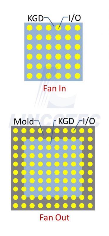
In the 1960s, IBM in the United States introduced the concept of chip connection in a flip-chip format. The process began by creating a wafer-level package (WLP) on the silicon wafer and designing metal bumps within the chip area, followed by using a Fan-In design, which formed metal bumps within the chip's range and metal solder on the bumps. The solder could melt and form spherical shapes, allowing for self-correcting for positioning when connecting chips to circuit boards based on their physical properties. This method improved yield and was used for products with fine pitch requirements. Flip-chip technology has advantages like high I/O density, electromagnetic shielding, low inductance, and compact packaging size, making it the most widely adopted packaging technology in the market.
Furthermore, in 2001, Infineon Technologies from Germany introduced the origin of fan-out wafer-level packaging (FOWLP) technology, as outlined in the US6727576B2patent. Quoting from SEMI, the description on their official website: "FOWLP technology involves drawing the needed circuitry from the endpoints of semiconductor wafers to the redistribution layer (RDL) to form packaging. Its most significant feature is that, for chips of the same size, the redistribution layer covers a wider range, allowing for more chip pins. A single chip can integrate more functions and achieve advantages such as substrate-less packaging, thinness, and cost-effectiveness. If high-density mass production is the goal, the application of redistribution layer technology will be critical."
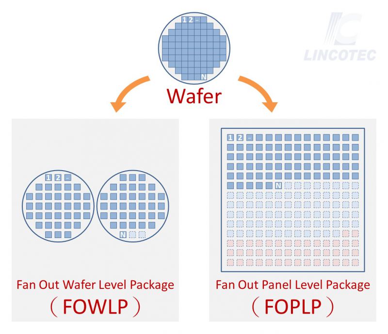
The FOWLP process can be divided into two main streams:
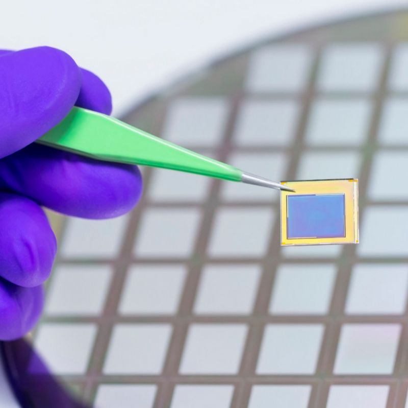
1.Chip-first Fan-Out: Chips (Know Good Die;KGD)from original device wafers are placed on a substrate, forming a reconstructed wafer with resin molding, followed by further processing into RDL on the wafer.
2.RDL-first Fan-Out: A carrier wafer's top end establishes the RDL layer and is temporarily bonded.
KGDs are placed on the top end, and then grinding and molding take place with the molds.
Fan-out wafer-level packaging technology is still based on front-end semiconductor processes. However, as it needs to provide space for routing lines outward, KGDs must be picked up and placed back (Pick and Place) onto the reconstructed wafer. Because front-end and back-end processes can be integrated, this technology, compared to other packaging methods, reduces production costs and material costs. It also meets high precision requirements for low line width and spacing (L/S), as it can integrate Stepper or Mask Aligners for high precision.
Not all chips require low line width and line spacing during packaging. In such cases, the key consideration becomes the selection of more versatile packaging materials and cost-effective equipment, which is the crucial factor of the PPAC index. In addition, each reconstructed wafer has a limited capacity for known good die (KGD), making it less suitable for large-scale one-time production. This limitation has given rise to the development of Fan-Out Panel Level Packaging (FOPLP), a fan-out packaging technology using larger rectangular carriers like printed circuit boards or glass substrates to facilitate fan-out packaging processes.
Both Fan-Out Wafer Level Packaging (FOWLP) and Fan-Out Panel Level Packaging (FOPLP) offer advantages such as improved electrical performance, increased I/O density, and support for thin and compact design. They are expected to further reduce production costs through the use of larger production areas, as seen in the capacity advantage when using FOPLP.
Here is a comparison of the characteristics of Fan-Out Wafer Level Packaging (FOWLP) and Fan-Out Panel Level Packaging (FOPLP):
| FOWLP | FOPLP | |
|---|---|---|
| FOWLP vs. FOPLP | FOWLP has limited capacity based on the size of the reconstructed wafer, resulting in lower production capacity. | In contrast, FOPLP has higher capacity, and when compared to FOWLP in 12-inch wafers, the single-carrier yield is approximately 7.8 times that of FOWLP. |
| Application Areas | FOWLP is suitable for chips with high I/O density requirements, such as CPUs, GPUs, APs, ASICs, FPGAs, AiPs, etc. | FOPLP is more appropriate for chips with lower I/O density requirements, such as PMICs, APEs, MEMS, sensors, and similar devices. |
| Equipment Requirements | FOWLP often requires more precise advanced process equipment, resulting in higher costs. | FOPLP has relatively lower precision equipment requirements, leading to lower costs. |
| Line Width/Line Spacing (L/S) | FOWLP typically has L/S < 5/5 | FOPLP has L/S ≥ 5/5. |
| RDL Layers | FOWLP can have five or more RDL layers | FOPLP is commonly used for four layers or fewer. |
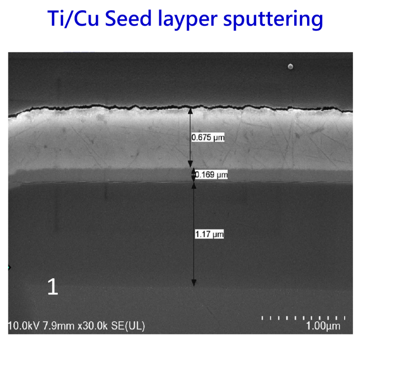
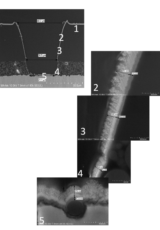
Lincotec possesses intellectual property and has the capability to collaborate with customers for process development and experimental validation, especially in the field of FOPLP. The company has rich experience in various technologies such as Desmear, Descum, Ti etching, and Seel layer sputtering, etc. Besides offering sampling services in the R&D phase with different process formulations, Lincotec has qualified and highly precise laboratories for sample testing.
Lincotec Features
Specialized in Sputter and Etching technologies, mastering key capabilities for FOPLP.
Achievements