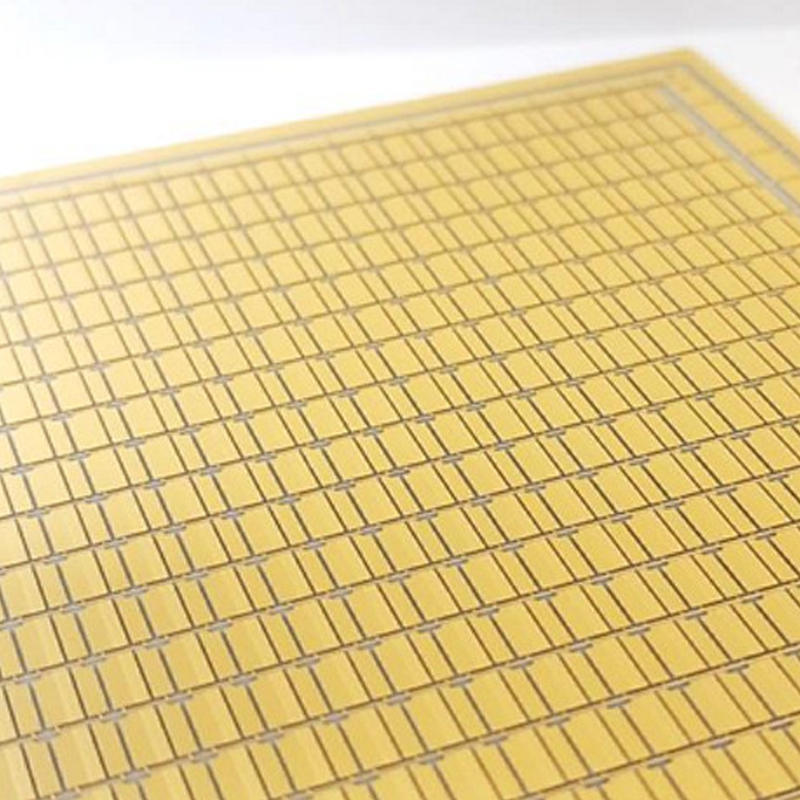
Backside metallization is a process used in the manufacturing of electronic devices where one or more layers of metal are deposited on the backside of a semiconductor substrate (such as a silicon wafer) or an integrated circuit (IC) using vacuum sputtering. These metal layers can serve as bonding/heat-conducting layers and can also bond with the substrate to improve heat dissipation, provide electromagnetic shielding, and reduce resistance.
The quality of the sputtering process in backside metallization has a significant impact on product yield and the reliability of semiconductor components. Poor bonding of the metal layer to the product can lead to issues like delamination and increased impedance. Low-ohmic contact resistance and excellent thin film adhesion are critical requirements for the backside metallization process.
Application Description
With the rapid advancement of technology, smart applications like 5G communication, Internet of Things (IoT), autonomous vehicles, advanced healthcare, and smart cities are flourishing. In this context, high-speed computing chips (High Performance Computing; HPC) used for high-speed computation and transmission have become indispensable. To address the issue with accumulated heat generated during these computations, Backside Metallization (BSM) products have emerged. BSM is achieved through two continuous processes, BG and BM. First, Backside Grinding (BG) involves thinning the substrate backside, reducing its thickness, and roughening the surface slightly. Then, one or more layers of metal (Backside Metallization; BM) are deposited as bonding or heat-conductive metal layers. The steps involved include:

Common seed layer materials include titanium (Ti) and chromium (Cr), while the metal layer mainly consists of aluminum (Al), copper (Cu), nickel (Ni), silver (Ag), gold (Au), or their combinations. Depending on the characteristics of the two metal layers, an intermediate layer may be deposited between the seed layer and the metal layer. For example, the back-end metallization of high-speed computing chips typically consists of a combination of titanium and gold layers, while the back-end metallization of power devices (Power Device) often comprises three layers: titanium layer (20-200nm) / nickel-tantalum alloy or pure nickel layer (200-400nm) / silver layer (100-2000nm). The titanium layer serves as the seed layer, the nickel-tantalum alloy or pure nickel layer acts as a diffusion barrier between the silicon substrate and the bonding material, and the silver layer ensures optimal solder wettability and prevents oxidation of the nickel layer before soldering.
Titanium as the bottom layer is widely used in back-end metallization technology to ensure high adhesion to the silicon substrate. However, the adhesion strength may inherently vary depending on wafer surface conditions, wafer surface pre-treatment techniques, and the parameters of thin-film sputtering processes. To reduce additional wafer warping, the sputtering process requires not only gentle and precise treatment but also effective stress control of the film stack, particularly in cases where chip stress distribution is uneven, leading to what is commonly known as ""potato cracking."" Additionally, to prevent thermal deformation of the thinned chips, in this process, it is necessary to improve the heat dissipation capabilities of the process since heating the wafer to enhance film adhesion is not an option. This, in turn, increases the complexity of equipment manufacturing.
The quality of the BSM sputtering process has a significant impact on product yield and the reliability of semiconductor components. Poor adhesion between the metal layer and the product can lead to issues such as metal layer delamination and increased impedance. Low ohmic contact resistance and excellent thin-film adhesion are the most critical requirements for the back-end metallization process.
In this regard, Lincotec, with its proprietary intellectual property, can collaborate with customers to develop processes and conduct experimental verifications. Particularly in the applications of back-end metallization processes, Lincotec has extensive experience in surface pre-treatment of wafers, low-temperature seed layer sputtering, and low-temperature metal layer sputtering, etc. In addition to offering prototyping services for various process formulations in the research and development phase, Lincotec also possesses qualified and highly precise laboratories for sample testing.