Every electronic component or system generates a certain level of electromagnetic
interference (EMI) during operation, which can adversely affect the performance of
nearby electronic devices. Therefore, EMI from electronic components or their systems
must be restricted, and they should also have sufficient immunity to environmental
interference.
"EMI shielding sputtering" is a dry process that involves physically deposit a
sufficient thickness of shielding material on the exterior of electronic components to
achieve electromagnetic shielding.
Application Description
"Electromagnetic Interference Shielding Sputtering" is the process of depositing a sufficiently thick layer of metal on the outer surface of electronic components. This is done to reduce electromagnetic interference generated by electronic components towards the external environment. It also prevents external electromagnetic interference from entering the internal components and affecting their operation. Many countries have established clear certification systems for electromagnetic standards, often based on the EMC (Electromagnetic Compatibility) standards defined by the International Electrotechnical Commission (IEC).
IEC's official website provides the following explanation for EMC:
「Every electrical and electronic device produces a certain level of so-called electromagnetic interference (EMI) that can adversely affect the performance of similar equipment located nearby.
Electromagnetic compatibility (EMC) provides methods that help contain EMI so that electrical and electronic systems or components are able to work correctly even when they are close together. In essence, EMC is about protecting sensitive equipment such as radio receivers, domestic appliances or electronic circuits from electromagnetic interference, and containing the electromagnetic emissions for example from large scale batteries, power lines or electric motors so that they can't interfere with more sensitive devices.
Multiple sources of electromagnetic disturbances can have a cumulative effect on a device. For example, the emissions from several laptop computers combined with those from mobile phones could disrupt systems in an aircraft.
The electromagnetic disturbances from each item of equipment must be limited and, simultaneously, each item must have an adequate level of immunity to the disturbances in its environment.」
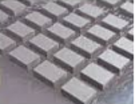
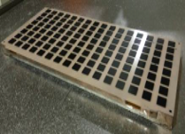
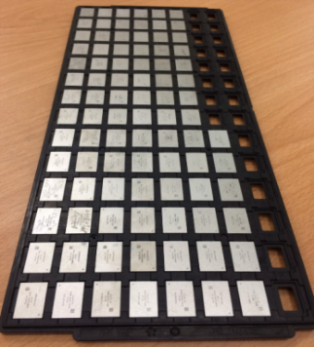
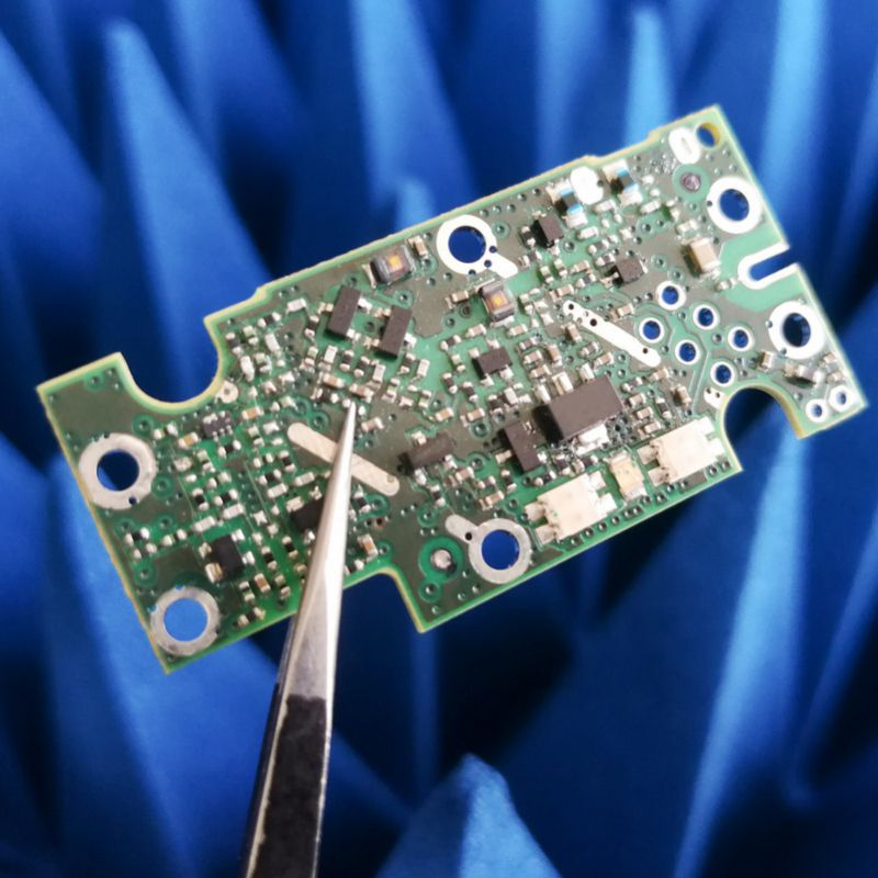
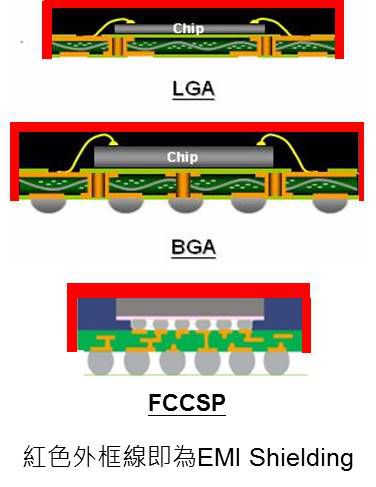
In general, equipment and electronic systems used in military or aerospace sectors have strict reliability requirements. Even in consumer electronic products like smartphones, televisions, digital cameras with communication capabilities like Wi-Fi or Bluetooth, in addition to applying electromagnetic interference shielding to their enclosures to comply with the certification standards mentioned above, further shielding is required for individual chip modules to reduce the occurrence of operational errors caused by electromagnetic interference between different chips or electronic components. For example, EMI shielding is applied to individual modules like Wi-Fi modules, Bluetooth modules, RF Front-End (RFFE) modules, and Power Management IC (PMIC) modules.
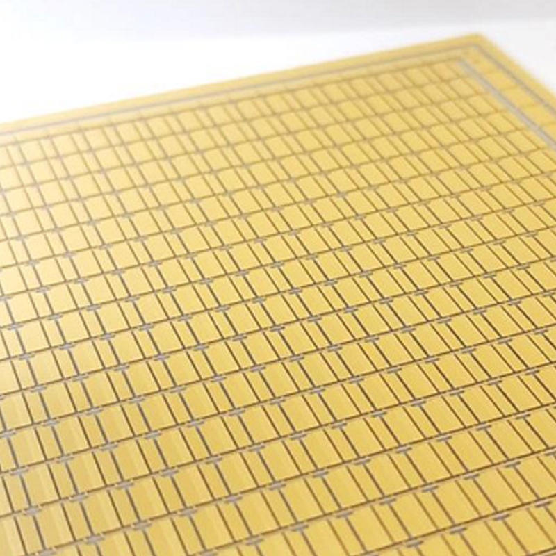
Sputtering process equipment, on the other hand, falls under the application of Physical Vapor Deposition (PVD) technology. It enables the preparation of uniform thin film coatings of high-melting-point materials in a vacuum environment and at lower temperatures through physical means. Especially as chips become increasinglyer, and various manufacturers work on reducing the spacing between adjacent electronic components, incorporating EMI shielding sputtering equipment during the System in Package (SiP) packaging process and applying a sufficiently thick shielding layer to the outer surfaces of electronic components in a dry, physical manner will be the most efficient and environmentally friendly choice in terms of productivity and effectiveness.
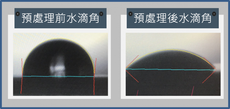
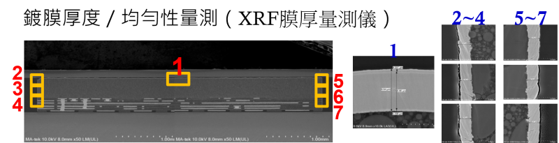
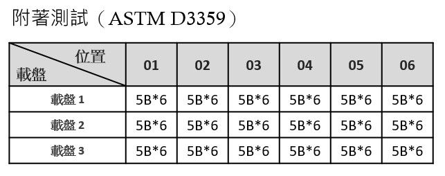
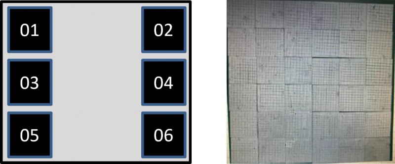
In this regard, the process validation for electromagnetic interference (EMI) shielding sputtering equipment should include at least the following: adhesion testing, measurement of film thickness uniformity, measurement of edge film thickness, coating resistance measurement, surface temperature limits for the substrate, Cpk, UPH, and target material utilization rate, etc. Furthermore, it is necessary to integrate the front and back-end processes to control the parameter characteristics of the substrate and provide excellent processing performance and stable reproducibility. Lincotec has rich intellectual property in the mentioned process validation, and possesses qualified and highly precise laboratories for sample testing, collaborating with customers in process development and experimental validation.
Lincotec Highlights
EMI sputtering equipment specified by world-renowned Tier 1 smartphone manufacturers.
Achievements